- 您现在的位置:买卖IC网 > Sheet目录345 > N02L6181AB27I (ON Semiconductor)IC SRAM 2MBIT 1.8V LP 48-BGA
N02L6181A
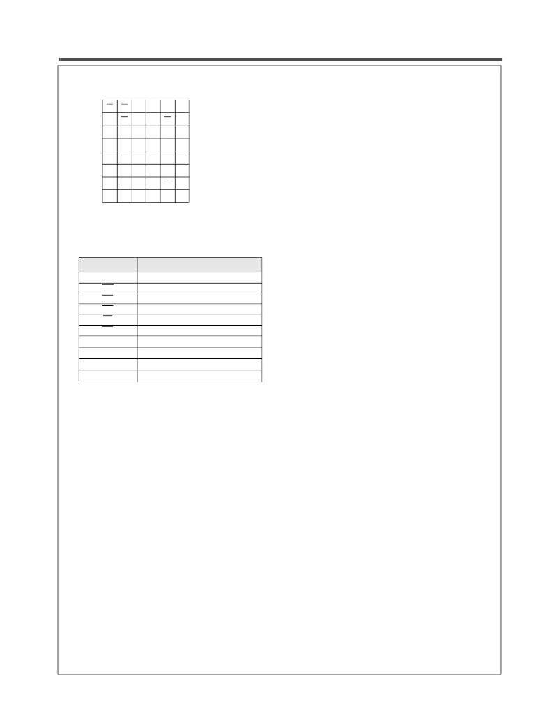
Pin Configurations
1
2
3
4
5
6
A
B
C
D
E
LB
I/O 8
I/O 9
V SS
V CC
OE
UB
I/O 10
I/O 11
I/O 12
A 0
A 3
A 5
NC
NC
A 1
A 4
A 6
A 7
A 16
A 2
CE
I/O 1
I/O 3
I/O 4
NC
I/O 0
I/O 2
V CC
V SS
F
I/O 14 I/O 13
A 14
A 15
I/O 5
I/O 6
G
H
I/O 15
NC
NC
A 8
A 12
A 9
A 13
A 10
WE
A 11
I/O 7
NC
48 Pin BGA (top)
6 x 8 mm
Pin Descriptions
Pin Name
A 0 -A 16
WE
CE
OE
LB
UB
I/O 0 -I/O 15
NC
V CC
V SS
Pin Function
Address Inputs
Write Enable Input
Chip Enable Input
Output Enable Input
Lower Byte Enable Input
Upper Byte Enable Input
Data Inputs/Outputs
Not Connected
Power
Ground
Rev. 4 | Page 2 of 11 | www.onsemi.com
发布紧急采购,3分钟左右您将得到回复。
相关PDF资料
N02L63W2AB25I
IC SRAM 2MBIT 3V LP 48-BGA
N02L63W3AT25IT
IC SRAM 2MBIT 3V LP 44-TSOP
N02L83W2AN25IT
IC SRAM 2MBIT 3V LP 32-STSOP
N04L63W1AB27I
IC SRAM 4MBIT 3V LP 48-BGA
N04L63W2AT27IT
IC SRAM 4MBIT 3V LP 44-TSOP
N050-012
PANEL PATCH CAT5E WALL MT 12PORT
N052-012
PANEL PATCH CAT5E 568B 12PORT
N052-024
PANEL PATCH CAT5E 568B 24PORT
相关代理商/技术参数
N02L6181AB27IT
制造商:ONSEMI 制造商全称:ON Semiconductor 功能描述:2Mb Ultra-Low Power Asynchronous CMOS SRAM 128Kx16 bit
N02L6181AB28I
功能描述:静态随机存取存储器 2MB 1.8V LOW PWR 静态随机存取存储器 RoHS:否 制造商:Cypress Semiconductor 存储容量:16 Mbit 组织:1 M x 16 访问时间:55 ns 电源电压-最大:3.6 V 电源电压-最小:2.2 V 最大工作电流:22 uA 最大工作温度:+ 85 C 最小工作温度:- 40 C 安装风格:SMD/SMT 封装 / 箱体:TSOP-48 封装:Tray
N02L6181AB28IT
制造商:ONSEMI 制造商全称:ON Semiconductor 功能描述:2Mb Ultra-Low Power Asynchronous CMOS SRAM 128Kx16 bit
N02L6181AB7I
制造商:ONSEMI 制造商全称:ON Semiconductor 功能描述:2Mb Ultra-Low Power Asynchronous CMOS SRAM 128Kx16 bit
N02L6181AB7IT
制造商:ONSEMI 制造商全称:ON Semiconductor 功能描述:2Mb Ultra-Low Power Asynchronous CMOS SRAM 128Kx16 bit
N02L6181AB8I
制造商:ONSEMI 制造商全称:ON Semiconductor 功能描述:2Mb Ultra-Low Power Asynchronous CMOS SRAM 128Kx16 bit
N02L6181AB8IT
制造商:ONSEMI 制造商全称:ON Semiconductor 功能描述:2Mb Ultra-Low Power Asynchronous CMOS SRAM 128Kx16 bit
N02L63W2A
制造商:ONSEMI 制造商全称:ON Semiconductor 功能描述:2Mb Ultra-Low Power Asynchronous CMOS SRAM 128K × 16 bit
